Thứ Bảy, 12 tháng 3, 2016

Harman/kardon DVD 50 – Circuit Diagram – Disassembly - 5 Disc DVD Changer

Applicable Discs: 5-inch (12cm) or 3-inch (8cm) DVD-Movie, CD, Video CD, MP3-CD, HDCD, CD-R or CD-RW discs.
Region 1 DVD-Movie discs
DVD: Single/Single Layer, Single Side/Dual Layer, Dual Side/Dual Layer
Linear PCM, Dolby Digital or DTS Audio
Video Signal System: NTSC
Composite Video Output: 1Vp-p/75 Ohms, sync, negative polarity
S-Video: Y/Liminace: 1Vp-p/75 Ohms, sync, negative polarity
C/Chrominance: 0.286Vp-p
Component Video Output: Y: 1Vp-p/75 Ohms, sync, negative polarity
Pr: 0.7Vp-p/75 Ohms
Pb: 0.7Vp-p/75 Ohms
Progressive Scan Output: Y: 1Vp-p/75 Ohms, sync, negative polarity
Pr: 0.7Vp-p/75 Ohms
Pb: 0.7Vp-p/75 Ohms
Analog Audio Output: HDCD: 2.0V RMS +/– 0.2V
Others: 1.0Vp-p RMS +/– 0.2V
Coaxial Digital Audio Output: 0.5Vp-p/75 Ohms
Frequency Response: 4Hz – 22kHz +/– 0.5dB (48kHz sampling)

AC Power: 100 – 240VAC 50/60Hz (Refer to back of the set.)
Power Consumption: 18 Watts
DISASSEMBLY
Tray Door
1.Eject the disc tray.
2.Lift up the tray door in the direction of the arrow.
Front Panel
1. Eject the disc tray. (See Fig. 2-2)
2. Remove the tray door. (See Fig. 2-2)
3. Pull the front panel toward you while pressing
5 stoppers to disengage, and remove the front panel.
CIRCUIT BOARD DISASSEMBLY
[Before removing the main circuit board, be sure to shortcircuit the laserdiode output land.  After replacing the main circuit board, open the land after inserting the flexible connector.]
Disassemble Main circuit board, Jack circuit board, Power circuit board and MD Ass'y DPM1.
1. Remove the top case. 
2. Remove 10 screws (B).
3. Disassemble Main circuit board and Jack circuit board from Bracket Main.
4. Unscrew 3 screws(C) at Bracket Main.
5. Disassemble Bracket Main from Main chassis.
6. Unscrew 4 screws(D) at MD Ass'y DPM1.
7. Turn the portion the direction of arrow to move the Base Assembly Tray in front of you.
8. Release the other 3 screws(E).
9. Disassemble MD Ass'y DPM1 from Main chassis.
10. Unscrew 4 screws(F) at Power circuit.
11. Disassemble power circuit board from Main chassis.
Digitron and Key Circuit Board
1. Remove the front panel. 
2. Release 5 screws (G), and remove the digitron circuit board.
Exploded view
DVD DSP SCHEMATIC
DRIVE AND RF SCHEMATIC
PANTERA SCHEMATIC
MEMORY SCHEMATIC
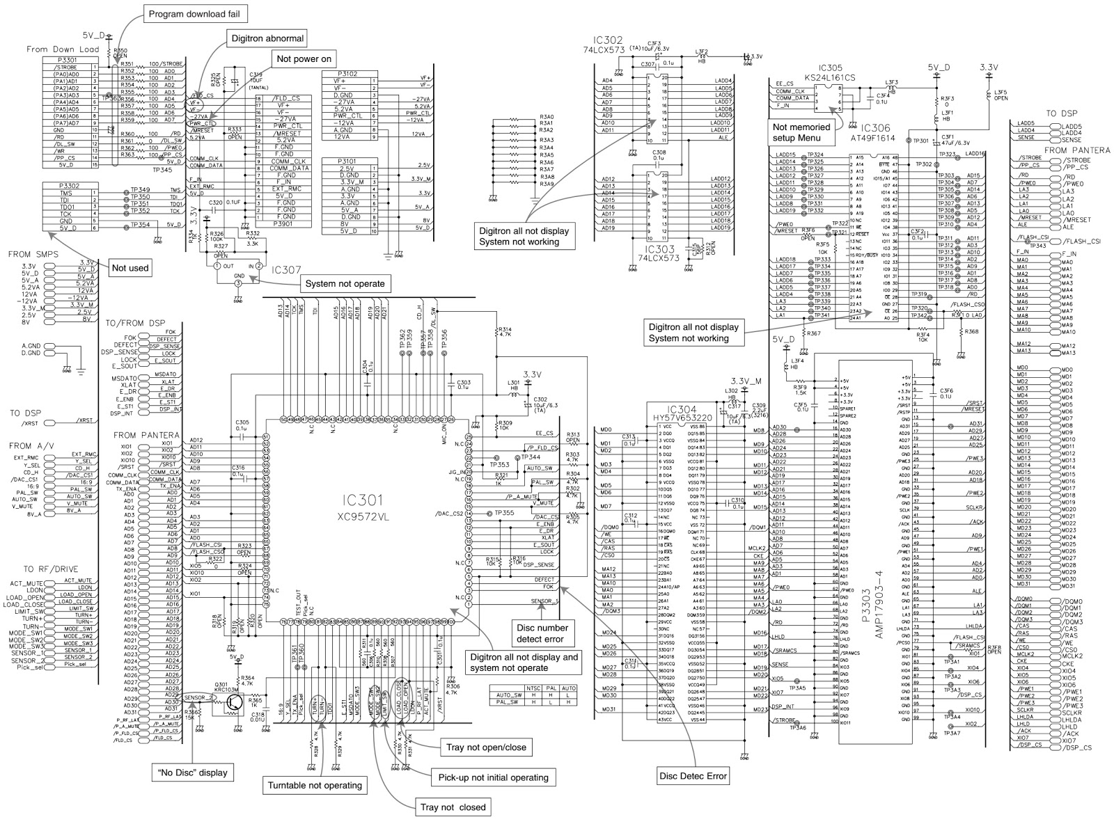
TIMER AND KEY SCHEMATIC
AV SCHEMATIC
AV JACK SCHEMATIC
Visit the previous post here to see the SMPS schematic
Click on the schematics to magnify

harman/kardon - DVD 26-28 – DVD 39-49 anf DVD 50 – 50 Five disc changer – SMPS Circuit Diagram

Power Supply Schematic – harman/kardon – DVD50 5 Disc changer – DVD26-28 – DVD39-49 – Harman/kardon DVD players
DVD 26 - 28 SMPS SCHEMATIC
DVD 39 - 49 SMPS SCHEMATIC
DVD 50 - 5 disc changer
Click on the schematic to zoom in

Thứ Tư, 9 tháng 3, 2016

Philips Plasma display FM23 - main digital board circuit diagram - 2

Scaler clock generator, PW scaler and memory, back end EPLD, Back end LVDS output, Audio source selection, Audio processor, Audio delay line
Scaler clock generator
PW Scaler and memory
Back end EPLD
Back end LVDS output
Audio source selection
Audio processor
Audio delay line

Philips FM 23 - Plasma Display - Main board Schematic -1

Sync selection and source selection, Video selection and matrix, Video selection ADC, Video selection decoder, VGA input, Control functions-1 & 2
Sync Selection and Source Selection
Video selection and matrix
Video selection ADC
Video selection decoder
VGA input
Control functions-1
Control functions-2
Click on the schematics to magnify

Thứ Sáu, 4 tháng 3, 2016

AOC AL512 – AOC AL513 – 15 Inch TFT LCD monitor – Circuit diagram

DC-DC CONVERTER
This block provides adjustable output voltages of 9.2V, -6V, 18V and 3 to 4V for the panel. It consists of a Q114 transistor and power switch IC I108 (AIC 1526-1). When DC_ EN signal is high, then Q114 is activated and send one signal to activate I108. At this time I108 will send 200KHz 12V PWM to Q106, Which is connected with L111, Q106, D203 and C308, to boost 5V to 9.2V. And I108 offers the adjustable voltage of 3V to 4V. By sending out pulses from pin 2 and pin 16 of I108 to double voltage circuit consisting of C301, D201, D202 and C303, leaner regulator with Q105, would output –6V, 18V output id created, according to the rule of –6V creation.
Inverter
In order to drive the CCFLs embedded in the panel module; there is a ROYER inverter to convert to convert the input 12V up to hundreds of AC voltage output.  The inverter is formed by symmetric, in order to drive the separate lamp modules.
The input stage consists of a PWM controller, buck choke, and switching MOSFET to convert DC input into AC output. The output stage consists of a tuning capacitor, transformer, push-pull transistor pair to boost ac output up to hundreds of voltage. And one resister is serial to lamp for output current feedback.  A 5-pin connector is the only interface to control the inverter. Pin 1 is 12V input, Pin 2/4 is the returns, pin3 is the control of output current, and pin 5 is the enable/disable control.
Audio Output
DC-DC converter
Panel Power
MCU
MVZ
Scalaring controller
MascotV scalar is a highly integrated solution that combines a high performance ADC with an advanced image processing controller. Using advanced image scaling algorithms, Mascot V has intelligently adaptive sub-algorithms that will automatically optimize the display quality for different images – the text is sharper and the graphics is smoother. The built-in analog interface includes a 160Mhz, 8-bit 3-channel ADC, preamplifier, and VGA, allowing seamless support to resolutions from VGA to XGA. MascotV also offers other integrated functions such as an internal OSD that supports all languages, and build-in line buffers that allows support to a wide range of LCD panels.  The scalar implements four advanced display technologies:
1. Sampling RGB input signals by fully integrated triple-channel ADC, PLL, and pre-amplifier
2. Automatically calibrate for vertical and horizontal alignment to center display and phase calibration
3. High-quality advanced scaling: Enhanced and adaptive scaling algorithm for optimal image quality
4. One and two pixels per clock panel support: Up to 24 bits per pixel.
The panel interface consists of 48-bit panel data bus, Start Pulse(STH1) and Clock (CLKH), Polarity(POL)/Latch pulse(LP) for source driver IC, Start pulse(STV1) and Clock(CLKV) for gate driver IC, and Data inversion control(HMSO/HMSE) for odd/even pixel bus and the power supply (+3.2V, +3.45V<adjustable>,+9.2V, +18Vand-6V) for panel driver IC use.

Thứ Năm, 3 tháng 3, 2016

Profolio PT100 – 100Hz CTV – Circuit diagram

ICs used: TDA4470 – TCDT1101G – TDA16846 – TDA6920 – MSP3411G – 74HCT86 – STU9379AF – TPU3050 – A42L2604 – TL7705 – CCU3000 – 27C2001 – TDA6111Q - VPC3230D – SDA9589X – MSM54V12222A – CTT5520E
CRT base card
POWER INPUT
PIP
MAIN BOARD
Click on the schematics to magnify

Thứ Tư, 2 tháng 3, 2016

Nad C 541i COMPACT DISC PLAYER – Circuit Diagram

PRECAUTIONS FOR CHECKING BEAM EMISSION
The laser beam of this unit is focused on the reflecting surface of the objective lens in the optical system block.  Therefore, keep your eyes at least 12 inches (30 cm) away from the objective lens when the laser diode is ON.  (Operation Check Method for Laser Diode and Focus Search Function.)
When the POWER switch is turned ON after the chucking plate is removed, observe the objective lens and confirm that the following operations are performed properly.
(The optical system should be at the lead-in area position when it is checked at this time.)
(1) The laser should be at the innermost position after the chucking plate is removed.
(2) The diffused light of the laser beam can be seen when the POWER switch is turned ON.
(3) Vertical (up and down) movement of the objective lens (2 or 3 times) will take place.
Click on the pictures to magnify
Main board
MCU 
Display
RF amplifier
Amplifier
Power
Wiring
Exploded view
When removing the pick-up assembly, short circuit the PCB tracks on the optical block as show in the drawing in order to protect the pick-up before removal.
NOTE: Replacement pick-up assemblies are supplied with the PCB pattern already protected.
DO NOT REMOVE THE SHORT CIRCUITS UNTIL YOU HAVE FINISHED FITTING THE PICK-UP.
Laser diodes are extremely susceptible to damage from static electricity. Even if a static discharge does not ruin the diode, it can shorten its life or cause it to work improperly. When replacing the pick-up, use a conductive mat, a grounded soldering iron, and so on, to protect the laser diode from static damage.